History
Early computers such as the ENIAC had to be physically rewired to perform different tasks, which caused these machines to be called "fixed-program computers". Since the term "CPU" is generally defined as a device for software (computer program) execution, the earliest devices that could rightly be called CPUs came with the advent of the stored-program computer.
The idea of a stored-program computer had been already present in the design of J. Presper Eckert and John William Mauchly's ENIAC, but was initially omitted so that it could be finished sooner. On June 30, 1945, before ENIAC was made, mathematician John von Neumann distributed the paper entitled First Draft of a Report on the EDVAC. It was the outline of a stored-program computer that would eventually be completed in August 1949. EDVAC was designed to perform a certain number of instructions (or operations) of various types. Significantly, the programs written for EDVAC were to be stored in high-speed computer memory rather than specified by the physical wiring of the computer. This overcame a severe limitation of ENIAC, which was the considerable time and effort required to reconfigure the computer to perform a new task. With von Neumann's design, the program that EDVAC ran could be changed simply by changing the contents of the memory. EDVAC, however, was not the first stored-program computer; the Manchester Baby, a small-scale experimental stored-program computer, ran its first program on 21 June 1948 and the Manchester Mark 1 ran its first program during the night of 16–17 June 1949.
Early CPUs were custom designs used as part of a larger and sometimes distinctive computer. However, this method of designing custom CPUs for a particular application has largely given way to the development of multi-purpose processors produced in large quantities. This standardization began in the era of discrete transistor mainframes and minicomputers and has rapidly accelerated with the popularization of the integrated circuit (IC). The IC has allowed increasingly complex CPUs to be designed and manufactured to tolerances on the order of nanometers. Both the miniaturization and standardization of CPUs have increased the presence of digital devices in modern life far beyond the limited application of dedicated computing machines. Modern microprocessors appear in electronic devices ranging from automobiles to cellphones, and sometimes even in toys.
While von Neumann is most often credited with the design of the stored-program computer because of his design of EDVAC, and the design became known as the von Neumann architecture, others before him, such as Konrad Zuse, had suggested and implemented similar ideas. The so-called Harvard architecture of the Harvard Mark I, which was completed before EDVAC, also used a stored-program design using punched paper tape rather than electronic memory. The key difference between the von Neumann and Harvard architectures is that the latter separates the storage and treatment of CPU instructions and data, while the former uses the same memory space for both. Most modern CPUs are primarily von Neumann in design, but CPUs with the Harvard architecture are seen as well, especially in embedded applications; for instance, the Atmel AVR microcontrollers are Harvard architecture processors.
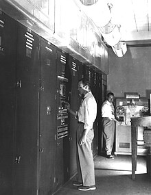
Relays and vacuum tubes (thermionic tubes) were commonly used as switching elements; a useful computer requires thousands or tens of thousands of switching devices. The overall speed of a system is dependent on the speed of the switches. Vacuum tube computers such as EDVAC tended to average eight hours between failures, whereas relay computers like the (slower, but earlier) Harvard Mark I failed very rarely. In the end, tube-based CPUs became dominant because the significant speed advantages afforded generally outweighed the reliability problems. Most of these early synchronous CPUs ran at low clock rates compared to modern microelectronic designs. Clock signal frequencies ranging from 100 kHz to 4 MHz were very common at this time, limited largely by the speed of the switching devices they were built with.
Transistor CPUsedit
The design complexity of CPUs increased as various technologies facilitated building smaller and more reliable electronic devices. The first such improvement came with the advent of the transistor. Transistorized CPUs during the 1950s and 1960s no longer had to be built out of bulky, unreliable and fragile switching elements like vacuum tubes and relays. With this improvement, more complex and reliable CPUs were built onto one or several printed circuit boards containing discrete (individual) components.
In 1964, IBM introduced its IBM System/360 computer architecture that was used in a series of computers capable of running the same programs with different speed and performance. This was significant at a time when most electronic computers were incompatible with one another, even those made by the same manufacturer. To facilitate this improvement, IBM used the concept of a microprogram (often called "microcode"), which still sees widespread usage in modern CPUs. The System/360 architecture was so popular that it dominated the mainframe computer market for decades and left a legacy that is still continued by similar modern computers like the IBM zSeries. In 1965, Digital Equipment Corporation (DEC) introduced another influential computer aimed at the scientific and research markets, the PDP-8.
Transistor-based computers had several distinct advantages over their predecessors. Aside from facilitating increased reliability and lower power consumption, transistors also allowed CPUs to operate at much higher speeds because of the short switching time of a transistor in comparison to a tube or relay. The increased reliability and dramatically increased speed of the switching elements (which were almost exclusively transistors by this time); CPU clock rates in the tens of megahertz were easily obtained during this period. Additionally, while discrete transistor and IC CPUs were in heavy usage, new high-performance designs like SIMD (Single Instruction Multiple Data) vector processors began to appear. These early experimental designs later gave rise to the era of specialized supercomputers like those made by Cray Inc and Fujitsu Ltd.
Small-scale integration CPUsedit
During this period, a method of manufacturing many interconnected transistors in a compact space was developed. The integrated circuit (IC) allowed a large number of transistors to be manufactured on a single semiconductor-based die, or "chip". At first, only very basic non-specialized digital circuits such as NOR gates were miniaturized into ICs. CPUs based on these "building block" ICs are generally referred to as "small-scale integration" (SSI) devices. SSI ICs, such as the ones used in the Apollo Guidance Computer, usually contained up to a few dozen transistors. To build an entire CPU out of SSI ICs required thousands of individual chips, but still consumed much less space and power than earlier discrete transistor designs.
IBM's System/370, follow-on to the System/360, used SSI ICs rather than Solid Logic Technology discrete-transistor modules. DEC's PDP-8/I and KI10 PDP-10 also switched from the individual transistors used by the PDP-8 and PDP-10 to SSI ICs, and their extremely popular PDP-11 line was originally built with SSI ICs but was eventually implemented with LSI components once these became practical.
Large-scale integration CPUsedit
The MOSFET (metal-oxide-semiconductor field-effect transistor), also known as the MOS transistor, was invented by Mohamed Atalla and Dawon Kahng at Bell Labs in 1959, and demonstrated in 1960. This led to the development of the MOS (metal-oxide-semiconductor) integrated circuit, proposed by Atalla in 1960 and Kahng in 1961, and then fabricated by Fred Heiman and Steven Hofstein at RCA in 1962. With its high scalability, and much lower power consumption and higher density than bipolar junction transistors, the MOSFET made it possible to build high-density integrated circuits.
Lee Boysel published influential articles, including a 1967 "manifesto", which described how to build the equivalent of a 32-bit mainframe computer from a relatively small number of large-scale integration circuits (LSI). The only way to build LSI chips, which are chips with a hundred or more gates, was to build them using a MOS semiconductor manufacturing process (either PMOS logic, NMOS logic, or CMOS logic). However, some companies continued to build processors out of bipolar transistor–transistor logic (TTL) chips because bipolar junction transistors were faster than MOS chips up until the 1970s (a few companies such as Datapoint continued to build processors out of TTL chips until the early 1980s). In the 1960s, MOS ICs were slower and initially considered useful only in applications that required low power. Following the development of silicon-gate MOS technology by Federico Faggin at Fairchild Semiconductor in 1968, MOS ICs largely replaced bipolar TTL as the standard chip technology in the early 1970s.
As the microelectronic technology advanced, an increasing number of transistors were placed on ICs, decreasing the number of individual ICs needed for a complete CPU. MSI and LSI ICs increased transistor counts to hundreds, and then thousands. By 1968, the number of ICs required to build a complete CPU had been reduced to 24 ICs of eight different types, with each IC containing roughly 1000 MOSFETs. In stark contrast with its SSI and MSI predecessors, the first LSI implementation of the PDP-11 contained a CPU composed of only four LSI integrated circuits.
Microprocessorsedit
Advances in MOS IC technology led to the invention of the microprocessor in the early 1970s. Since the introduction of the first commercially available microprocessor, the Intel 4004 in 1971, and the first widely used microprocessor, the Intel 8080 in 1974, this class of CPUs has almost completely overtaken all other central processing unit implementation methods. Mainframe and minicomputer manufacturers of the time launched proprietary IC development programs to upgrade their older computer architectures, and eventually produced instruction set compatible microprocessors that were backward-compatible with their older hardware and software. Combined with the advent and eventual success of the ubiquitous personal computer, the term CPU is now applied almost exclusivelya to microprocessors. Several CPUs (denoted cores) can be combined in a single processing chip.
Previous generations of CPUs were implemented as discrete components and numerous small integrated circuits (ICs) on one or more circuit boards. Microprocessors, on the other hand, are CPUs manufactured on a very small number of ICs; usually just one. The overall smaller CPU size, as a result of being implemented on a single die, means faster switching time because of physical factors like decreased gate parasitic capacitance. This has allowed synchronous microprocessors to have clock rates ranging from tens of megahertz to several gigahertz. Additionally, the ability to construct exceedingly small transistors on an IC has increased the complexity and number of transistors in a single CPU many fold. This widely observed trend is described by Moore's law, which had proven to be a fairly accurate predictor of the growth of CPU (and other IC) complexity until 2016.
While the complexity, size, construction and general form of CPUs have changed enormously since 1950, the basic design and function has not changed much at all. Almost all common CPUs today can be very accurately described as von Neumann stored-program machines.b As Moore's law no longer holds, concerns have arisen about the limits of integrated circuit transistor technology. Extreme miniaturization of electronic gates is causing the effects of phenomena like electromigration and subthreshold leakage to become much more significant. These newer concerns are among the many factors causing researchers to investigate new methods of computing such as the quantum computer, as well as to expand the usage of parallelism and other methods that extend the usefulness of the classical von Neumann model.

Comments
Post a Comment